
A Importância Crítica de Sala limpa Ambientes na Fabricação de Semicondutores
Controle de Partículas em Níveis Sub-Micrônicos
No fabrico de semicondutores, controlar partículas sub-micrônicas é um fator crucial que influencia tanto as taxas de produção quanto o desempenho do dispositivo. Devido à natureza delicada dos semicondutores, até uma única partícula microscópica pode causar defeitos que custam aos fabricantes milhões. As salas limpas são projetadas para alcançar níveis de contaminação significativamente abaixo de 0,1 micrômetros, garantindo que a integridade do Produtos seja mantida. Esses ambientes dependem de sistemas avançados de filtração de ar, como filtros HEPA e ULPA, para manter o nível de limpeza necessário.
Estudos da indústria destacam o impacto considerável da contaminação por partículas. Por exemplo, defeitos causados por contaminação sub-micrométrica podem resultar em perdas financeiras substanciais, com algumas estimativas colocando o custo em milhões de dólares por incidente. Os altos padrões de limpeza exigidos nos salas limpas de semicondutores demonstram tanto os desafios quanto a importância de manter um ambiente livre dessas partículas.
Classificações ISO e Taxas de Produção de Semicondutores
As classificações ISO, especificamente a ISO 14644, têm um impacto direto nas taxas de produção na fabricação de semicondutores. Esses padrões categorizam as salas limpas pelo número de partículas por metro cúbico, influenciando os ambientes de produção da Classe 1 à Classe 100. Cada classificação corresponde a processos de fabricação específicos dentro da indústria de semicondutores. Por exemplo, o processo de fotolitografia geralmente ocorre em um ambiente de sala limpa Classe 1 para evitar qualquer interferência de partículas, otimizando assim as taxas de produção.
O cumprimento desses padrões rigorosos é fundamental para aumentar as taxas de produção e a qualidade do produto. Empresas de semicondutores como Intel e TSMC implementaram padrões ISO rigorosos, garantindo uma contaminação mínima e uma eficiência de produção aprimorada. Dados dessas empresas indicam uma melhoria significativa nas taxas de rendimento e na qualidade geral dos semicondutores, destacando a importância de manter padrões de sala limpa no processo de fabricação.
Impactos Econômicos de Violações de Contaminação
As repercussões econômicas das violações de contaminação em fábricas de semicondutores podem ser catastróficas. Tais incidentes muitas vezes levam a custos de retrabalho, perdas de produção e, potencialmente, perdas significativas de participação de mercado. Relatórios da indústria revelam que o custo médio de um evento de contaminação pode chegar a milhões, afetando severamente o resultado financeiro de uma empresa. Além disso, os impactos de longo prazo não se limitam a perdas financeiras, mas também incluem danos à reputação e redução nas taxas de retenção de clientes.
A reputação e a confiabilidade são fundamentais em um setor onde a precisão e a qualidade não são negociáveis. A contaminação pode danificar ambos, levando os clientes a buscarem parceiros mais confiáveis. Isso torna a manutenção de procedimentos rigorosos de limpeza e controle não apenas uma questão de boa prática, mas um componente crítico para sustentar a viabilidade econômica e a vantagem competitiva no mercado de semicondutores.
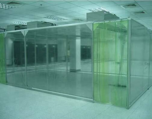
Benefícios dos Laboratórios Limpos Modulares para Instalações de Semicondutores
Escalabilidade para Processos de Fabricação em Evolução
Sala limpa modular oferece escalabilidade e adaptabilidade, tornando-a invaluable para a indústria de fabricação de semicondutores em rápida evolução. À medida que os nós tecnológicos avançam e os processos de fabricação exigem ajustes, designs modulares permitem expansões e modificações sem uma interrupção substancial. Por exemplo, vários fabricantes atualizaram com sucesso suas instalações de salas limpas para acomodar as mais recentes tecnologias por meio de soluções modulares. Estudos de caso de várias instalações de semicondutores destacam como essas salas limpas modulares facilitaram transições suaves, garantindo que suas capacidades de produção acompanhem os avanços da indústria.
Capacidades de Reconfiguração Custo-Efetivas
Uma das vantagens mais notáveis das salas limpas modulares é sua eficiência de custo, especialmente ao reconfigurar layouts para diferentes linhas de produção. Ao contrário das salas limpas tradicionais, que muitas vezes incorrem em altos custos de construção e operação, as salas limpas modulares reduzem significativamente esses gastos. Estudos mostraram que empresas que implementam designs modulares enfrentam custos mais baixos tanto na construção quanto na operação a longo prazo, permitindo alocação estratégica de recursos. Consequentemente, essas economias se traduzem em uma melhoria do resultado final, pois as instalações podem gerenciar eficientemente seus recursos financeiros enquanto mantêm ambientes de produção flexíveis.
Implantação Rápida em Instalações Existentes
O design modular acelera significativamente o processo de implantação, permitindo que instalações semicondutoras fiquem operacionais rapidamente e com mínima perturbação. Em edifícios existentes, salas limpas modulares são instaladas em prazos muito mais curtos em comparação com métodos de construção convencionais. Por exemplo, várias empresas semicondutoras alcançaram tempos de configuração rápidos ao utilizarem soluções modulares, evitando assim tempos de inatividade prolongados. Essa capacidade de atualizar ou expandir instalações rapidamente garante que os processos produtivos permaneçam ininterruptos, aumentando a eficiência e produtividade geral das operações de fabricação de semicondutores.
Inovações no Design de Tecnologia Modular de Sala Limpa
Unidades Avançadas de Tratamento de Ar para Controle de Precisão
Unidades modernas de tratamento de ar desempenham um papel crucial na manutenção de rigorosos padrões de qualidade do ar dentro de salas limpas. Essas unidades são equipadas com recursos avançados, como alta eficiência de filtração e mecanismos precisos de controle de fluxo de ar, que são essenciais para controlar o ambiente da sala limpa. Avanços recentes incluem filtros HEPA aprimorados e sistemas de controle inteligente que garantem a qualidade do ar ótima e previnem contaminações. Em designs de salas limpas para semicondutores, essas inovações são cruciais para manter os elevados padrões de limpeza necessários para processos de fabricação sensíveis. Tais avanços demonstram a eficácia e a necessidade dessas unidades na obtenção de controle de precisão em ambientes de salas limpas.
Soluções de Sala Limpa Móvel para Operações Flexíveis
As salas limpas móveis oferecem uma flexibilidade sem igual para diversas necessidades de produção, adaptando-se facilmente a diferentes processos de fabricação. Essas soluções são particularmente benéficas em ambientes de pesquisa e desenvolvimento, onde facilitam a prototipagem e testes iterativos sem as limitações impostas por instalações estáticas. As salas limpas móveis ganharam força na indústria devido à sua capacidade de serem rapidamente implantadas e reconfiguradas conforme necessário. Além disso, elas permitem que os fabricantes respondam a demandas em mudança de forma fluida, tornando-as um ativo inestimável para empresas que priorizam a adaptabilidade operacional.
Materiais Conformes ao ESD para Ambientes Sensíveis a Estática
A necessidade de materiais conformes com ESD em ambientes de sala limpa é fundamental para proteger dispositivos semicondutores sensíveis de descargas estáticas. Estratégias comuns incluem o uso de pisos aterrados, superfícies de trabalho dissipativas de estática e roupas condutoras, que se tornaram padrão nos designs de salas limpas devido à sua eficácia na mitigação dos riscos de ESD. Essas medidas reduzem significativamente as taxas de falha associadas a incidentes de descarga estática, garantindo a integridade do dispositivo. Dados apoiam que tais precauções levam a uma diminuição notável nas falhas de componentes eletrônicos, destacando sua importância em ambientes sensíveis à estática. Integrar materiais conformes com ESD agora é uma consideração crítica no design de qualquer sala limpa destinada à indústria semicondutora.
Integração com Processos de Fabricação de Semicondutores
Controles Ambientais Compatíveis com Fotolitografia
Na fabricação de semicondutores, a fotolitografia é crucial, exigindo controles ambientais precisos, especialmente temperatura e umidade. Esses parâmetros afetam diretamente os resultados da produção; portanto, uma regulação rigorosa é necessária para minimizar defeitos e otimizar o rendimento. Por exemplo, manter níveis de umidade entre 40-50% pode prevenir problemas relacionados à umidade durante o processo de fotoresistência Aplicação , garantindo padrões mais nítidos e menos erros. Semicondutores também precisam de faixas de temperatura específicas para evitar falhas que podem ocorrer devido à expansão térmica dos disco (wafers). Ao seguir as especificações do fabricante para esses controles, salas limpas podem melhorar a eficiência da produção e reduzir as taxas de defeitos, aumentando o sucesso operacional.
Sistemas de Piso Elevado para Distribuição de Serviços
Sistemas de piso elevado fornecem vantagens significativas em instalações de semicondutores, particularmente para distribuição de utilidades e gerenciamento de fluxo de ar. Esses sistemas suportam uma circulação de ar eficiente, crucial para manter a limpeza e condições ambientais consistentes. Pisos elevados também oferecem acesso mais fácil a fiação e encanamento, evitando interrupções e garantindo o ambiente impecável necessário para a produção de semicondutores. Essa acessibilidade não compromete a limpeza, pois pisos selados impedem que contaminantes infiltrem-se em áreas sensíveis. Estatisticamente, instalações com sistemas de piso elevado implementados relatam uma eficiência operacional aprimorada, com custos de manutenção reduzidos e aumento na capacidade de produção devido ao acesso simplificado à infraestrutura.
Modo Noturno HVAC para Eficiência Energética
O modo noturno do HVAC é uma estratégia inovadora para melhorar a eficiência energética em fábricas de semicondutores, especialmente durante as horas não operacionais. Ajustando as configurações de temperatura e fluxo de ar, esses sistemas reduzem significativamente o consumo de energia enquanto mantêm proteção adequada para equipamentos sensíveis. Várias fábricas de semicondutores implementaram com sucesso o modo noturno do HVAC, demonstrando economias substanciais. Análises da indústria revelam que esses sistemas podem reduzir o consumo de energia em até 15%, exemplificando benefícios financeiros e ambientais significativos. Garantindo condições de temperatura ótimas sem o uso excessivo de energia, as instalações mantêm a eficiência operacional enquanto reduzem custos e aumentam a sustentabilidade.
Estudos de Caso: Sucesso Modular na Produção de Semicondutores
Instalação no Arizona: Design Dual-Purpose de P&D/Fabricação
A instalação no Arizona representa um exemplo quintessencial de utilização do design de sala limpa modular para fins duplos de P&D e fabricação. Este design inovador permite transições suaves entre a pesquisa e a produção em larga escala, otimizando ambos os espaços para necessidades operacionais específicas. Como resultado, a instalação presenciou melhorias significativas nos indicadores de produção, destacando a versatilidade e eficiência dessa abordagem modular. Estatísticas pós-implementação revelam um crescimento notável na saída de produção, alinhando-se com os objetivos estratégicos de maior adaptabilidade e eficácia operacional.
Conversão de Fábrica de Alto Volume Usando Módulos Pré-Fabricados
Uma fábrica de semicondutores de alto volume utilizou com sucesso a pré-fabricação modular para maximizar a eficiência e a capacidade de produção. Ao incorporar módulos pré-fabricados em seu processo de fabricação, a fábrica atingiu uma conversão rápida para a produção em grande escala. O processo de conversão foi meticulosamente planejado, com um cronograma bem definido que abordou desafios potenciais, como a integração de novos módulos e a manutenção da continuidade na produção. Dados após a conversão indicam aumentos substanciais tanto na produção quanto na eficiência operacional, confirmando a eficácia de estratégias modulares no manejo de demandas de produção substanciais.
Salas Limpas Móveis para Prototipagem de Equipamentos
As salas limpas móveis revolucionaram o prototipagem de equipamentos ao oferecerem uma versatilidade sem igual e adaptabilidade no local. Essas salas limpas facilitam a prototipagem em diferentes locações, atendendo às demandas únicas de cada projeto com facilidade. Vários estudos de caso destacam a eficácia das soluções móveis, demonstrando reduções significativas nos prazos de prototipagem e aumento da eficiência dos projetos. Ao oferecer um ambiente controlado independentemente do local, as salas limpas móveis garantem que os processos de prototipagem sejam realizados rapidamente sem comprometer a qualidade ou a limpeza.
Protegendo o Futuro das Salas Limpas de Semicondutores
Sistemas de Monitoramento Inteligente para Validação em Tempo Real
Sistemas de monitoramento inteligente estão se tornando um componente crucial na validação em tempo real das condições de salas limpas de semicondutores. Essas tecnologias fornecem vigilância constante e feedback de dados instantâneo para manter parâmetros ambientais, cruciais para os processos de fabricação altamente sensíveis. Avanços na automação permitiram que esses sistemas garantam uma estrita conformidade com os padrões de limpeza estabelecidos, reduzindo eficazmente os erros humanos. Empresas como Intel e Samsung implementaram com sucesso sistemas de monitoramento em tempo real, otimizando seus processos de sala limpa. Por exemplo, dados em tempo real levaram à manutenção proativa e reduziram o tempo de inatividade, aumentando ultimate a eficiência e qualidade da produção.
Filtragem Adaptativa para Fabricação de Nós de Próxima Geração
Tecnologias de filtração adaptativa surgiram como instrumentais no avanço dos processos de fabricação de nós para semicondutores. Esses sistemas se adaptam a condições ambientais variáveis, otimizando assim a filtração de partículas. Evidências mostram que a filtração adaptativa captura eficazmente até os contaminantes mais elusivos, garantindo a pureza na produção. Um exemplo notável no mercado seria a redução de partículas submicrônicas nas instalações da TSMC, melhorando o desempenho dos dispositivos semicondutores. Essas melhorias na filtração de ar correlacionam-se diretamente com aumentos na produtividade e redução nas taxas de defeitos, escalando as operações para a fabricação de nós de próxima geração.
Materiais Sustentáveis na Construção Modular
A indústria de semicondutores está testemunhando um crescimento no uso de materiais sustentáveis na construção de salas limpas modulares. Essa tendência é impulsionada pela meta da indústria de aumentar a responsabilidade ambiental enquanto mantém os mais altos padrões de sala limpa. Materiais específicos, como alumínio reciclado e tintas com baixo teor de COV, estão agora sendo incorporados, garantindo conformidade com importantes benchmarks de sustentabilidade. A introdução desses materiais está alinhada com as chamadas globais por práticas mais verdes, evidenciada pela redução das pegadas de carbono em toda a indústria. Dados indicam um aumento anual de 15% nas instalações ecológicas, moldando um novo padrão de responsabilidade ambiental na construção de salas limpas.
Perguntas Frequentes
Qual é a importância do controle de partículas na fabricação de semicondutores?
O controle de partículas é crucial porque até uma única partícula microscópica pode levar a defeitos em semicondutores, influenciando as taxas de produção e o desempenho do dispositivo. Salas limpas são projetadas para minimizar a contaminação, garantindo a integridade do produto.
Como as classificações ISO impactam as taxas de produção de semicondutores?
As classificações ISO, como a ISO 14644, categorizam salas limpas por densidade de partículas, afetando as taxas de produção. Adotar esses padrões ajuda a otimizar os processos de fabricação, melhorando assim as taxas de produção e a qualidade do produto.
Por que as salas limpas modulares são benéficas para instalações de semicondutores?
As salas limpas modulares oferecem escalabilidade, custo-efetividade e implantação rápida, permitindo que instalações de semicondutores evoluam com os avanços tecnológicos sem interrupções substanciais.
Índice
- A Importância Crítica de Sala limpa Ambientes na Fabricação de Semicondutores
- Benefícios dos Laboratórios Limpos Modulares para Instalações de Semicondutores
- Inovações no Design de Tecnologia Modular de Sala Limpa
- Integração com Processos de Fabricação de Semicondutores
- Estudos de Caso: Sucesso Modular na Produção de Semicondutores
- Protegendo o Futuro das Salas Limpas de Semicondutores
- Perguntas Frequentes